Samsung Accelerates HBM4 Production to Meet Nvidia's Growing AI Demand
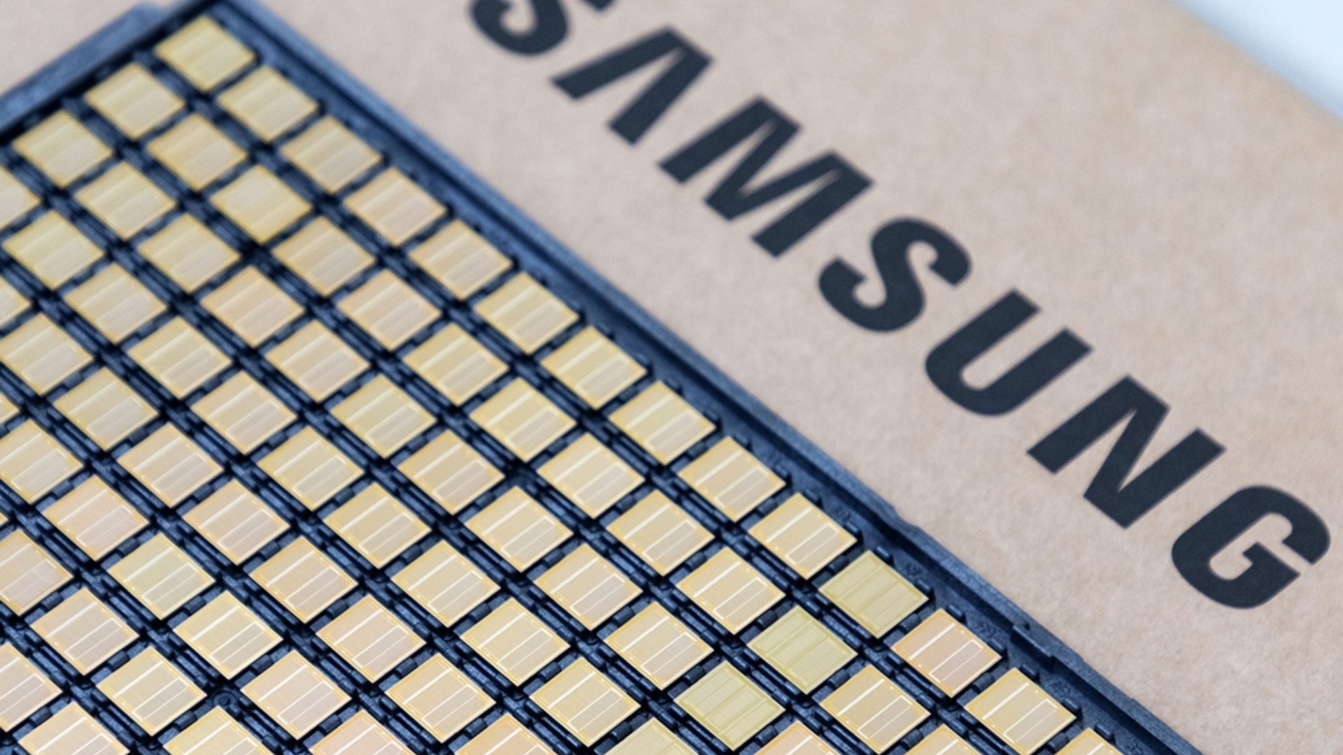
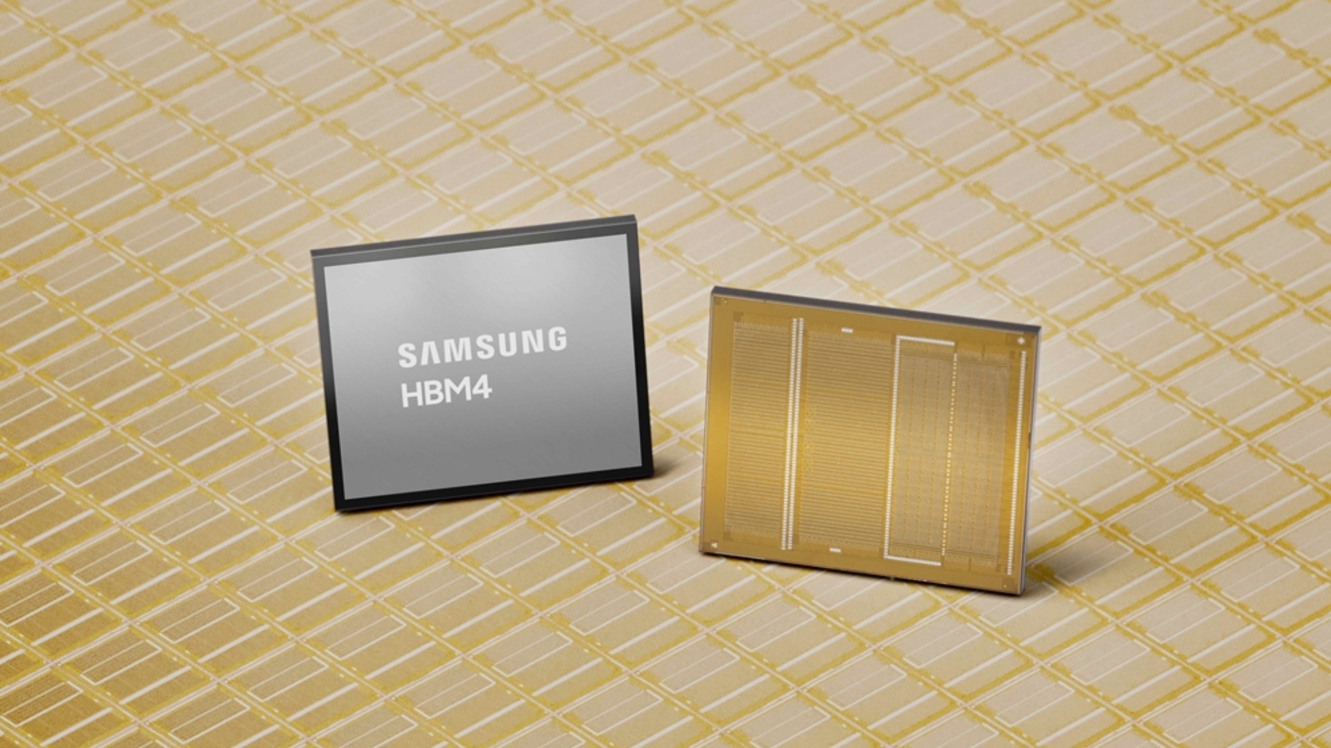
Samsung Electronics has officially entered the mass production phase for its sixth-generation high-bandwidth memory, known as HBM4. By achieving this milestone, the South Korean tech giant has secured its position as the first company globally to reach this level of manufacturing for the latest memory standard. To further cement its lead, Samsung is now reportedly fast-tracking the deployment of advanced semiconductor packaging technologies at its specialized facility in Cheonan, South Korea.
- ✨ Samsung is the first in the world to begin mass production of sixth-generation HBM4 chips.
- ✨ A new Hybrid Copper Bonding (HCB) line is being established to shorten delivery timelines.
- ✨ The HCB technology is expected to reduce thermal resistance by approximately 20%.
- ✨ Production schedules were moved forward following specific requests from Nvidia.
- ✨ Samsung is preparing for future generations, including HBM4E and HBM5.

Deployment of HCB Packaging Equipment in Cheonan
A recent report indicates that Samsung is currently setting up a Hybrid Copper Bonding (HCB) production line specifically for its HBM lineup. This strategic move is designed to minimize production bottlenecks and drastically reduce the time it takes to deliver Samsung Memory products to major clients. By optimizing the packaging process, Samsung aims to stay ahead of the curve for upcoming iterations like HBM4E and HBM5.
The necessary machinery for the HCB line is slated to arrive at the Cheonan plant this March. Once installed, the equipment will undergo rigorous testing to verify the quality and reliability of the packaged semiconductors. Full-scale manufacturing is expected to commence immediately after the initial validation phase. Interestingly, industry sources suggest that Samsung accelerated this timeline specifically to meet the urgent requirements of Nvidia, the leader in the AI GPU market.
Understanding HCB Packaging and Its Benefits

High-bandwidth memory chips are constructed by vertically stacking multiple memory dies. As these stacks grow taller to accommodate more data, the physical thickness of the chip increases, leading to higher heat generation. Efficient thermal management is the biggest challenge in modern chip design, necessitating a leap in packaging technology.
Hybrid Copper Bonding (HCB) addresses this by enhancing the electrical and physical links between the stacked layers. Samsung’s technical leadership has noted that HCB can lower thermal resistance by as much as 20%. While these results are impressive in a lab setting, the industry is now watching to see if Samsung can replicate these gains in mass production while maintaining high yields and cost-effectiveness.
The Growing Complexity of HBM Technology

The competition between major players like Samsung, SK Hynix, and Micron has shifted. While bandwidth and data transfer speeds remain vital, the focus is now expanding toward power efficiency, production stability, and thermal dissipation. As HBM chips become more integral to AI accelerators, the ability to manufacture them reliably at scale is the new frontier of the semiconductor war.
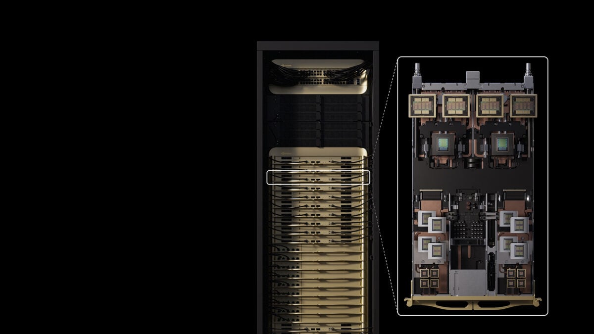
The tech world is eager to see how Samsung’s HBM4 chips will perform when integrated into next-generation AI hardware, such as Nvidia’s Rubin architecture or AMD’s MI450. Success in this area could redefine Samsung's dominance in the high-end memory market for years to come.
What exactly is HBM4 and why is it important for AI?
HBM4 is the sixth generation of high-bandwidth memory. It is crucial for AI because it provides the massive data speeds required by modern GPUs to process complex artificial intelligence models efficiently without creating performance bottlenecks.
How does Hybrid Copper Bonding (HCB) improve chip performance?
HCB improves performance by creating better electrical connections and reducing the distance between stacked layers. This results in a 20% reduction in thermal resistance, allowing the chips to run cooler even under heavy workloads.
Why is Nvidia requesting Samsung to speed up production?
Nvidia is the global leader in AI hardware. With the rapid expansion of AI services, the demand for high-performance memory has outpaced supply. Nvidia needs Samsung to boost production to ensure their next-generation AI accelerators can be shipped to customers on time.
Where is Samsung producing these new HBM4 chips?
Samsung is producing and packaging these advanced chips at its specialized semiconductor facility located in Cheonan, South Chungcheong Province, South Korea.
What are the challenges of mass-producing HCB-packaged chips?
The primary challenges include maintaining a high manufacturing yield (the percentage of functional chips per wafer), ensuring long-term reliability of the copper bonds, and keeping production costs low enough for commercial viability.
🔎 In conclusion, Samsung's aggressive push into HBM4 mass production and the implementation of HCB packaging technology represent a pivotal moment in the semiconductor industry. By responding directly to the needs of AI giants like Nvidia, Samsung is not just selling components but is actively shaping the infrastructure of the future. As AI models continue to grow in complexity, the innovations happening today at the Cheonan plant will likely determine the pace of technological progress for the entire artificial intelligence ecosystem.

Post a Comment