
Samsung Reclaims the AI Throne: Mass Production of Next-Gen HBM4 Chips Officially Begins
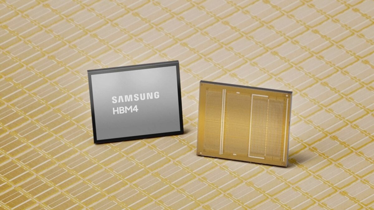
Samsung Electronics has officially announced a monumental shift in the semiconductor landscape, becoming the first company in the world to initiate mass production of its sixth-generation high-bandwidth memory, known as HBM4. This breakthrough represents more than just a technical upgrade; it is a strategic move to power the most sophisticated AI accelerators on the planet and re-establish the company’s dominance in the high-performance memory market.
Article Summary:
Samsung has leapfrogged competitors by launching HBM4 mass production using cutting-edge 1c DRAM and 4nm foundry technology. These chips offer a massive 46% speed increase over industry standards, specifically designed to meet the extreme demands of the global AI revolution.
- ✨ World’s first mass production of sixth-generation HBM4 memory modules.
- ✨ Utilizes advanced 1c DRAM and 4nm fabrication for peak efficiency.
- ✨ Achieve speeds of 11.7Gbps, significantly outpacing JEDEC standards.
- ✨ Roadmap includes HBM4E in late 2026 and custom HBM solutions by 2027.
Bridging the Gap: Samsung’s Return to Market Leadership
The announcement of HBM4 mass production marks a pivotal "return to form" for Samsung Electronics. After facing stiff competition and falling slightly behind rivals like Micron and SK Hynix last year, the South Korean tech giant is now leading the charge. By integrating its most advanced **high-bandwidth memory** technology, Samsung is positioning itself as the primary supplier for the next wave of **AI accelerators**.
Central to this achievement is the use of 1c DRAM technology. This 10nm-class, sixth-generation manufacturing process is currently the most sophisticated in the industry. Furthermore, Samsung has employed a 4nm fabrication process to enhance performance and power efficiency, ensuring that they can provide stable yields to meet the massive global demand for AI processing power.
Breaking Speed Records and Capacity Barriers
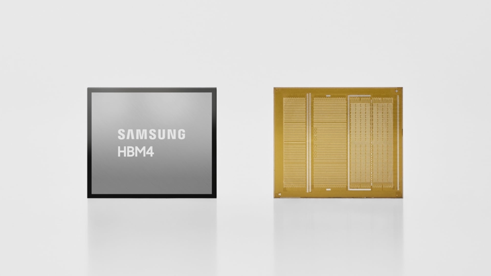
Performance metrics for the new HBM4 chips are staggering. Operating at 11.7Gbps, these chips are 46% faster than the JEDEC industry standard of 8Gbps and 22% faster than Samsung’s own fifth-generation HBM3E. With a single stack reaching a total memory bandwidth of 3.3TB/s, Samsung has officially exceeded the 3TB/s threshold typically requested by high-end enterprise clients.
Samsung is currently shipping HBM4 chips in capacities ranging from 24GB to 36GB. However, the company isn't stopping there. To satisfy the hunger of massive Large Language Models (LLMs), Samsung plans to introduce 16-layer HBM4 chips with capacities reaching up to 48GB in the near future.
The Future Roadmap: HBM4E and Beyond
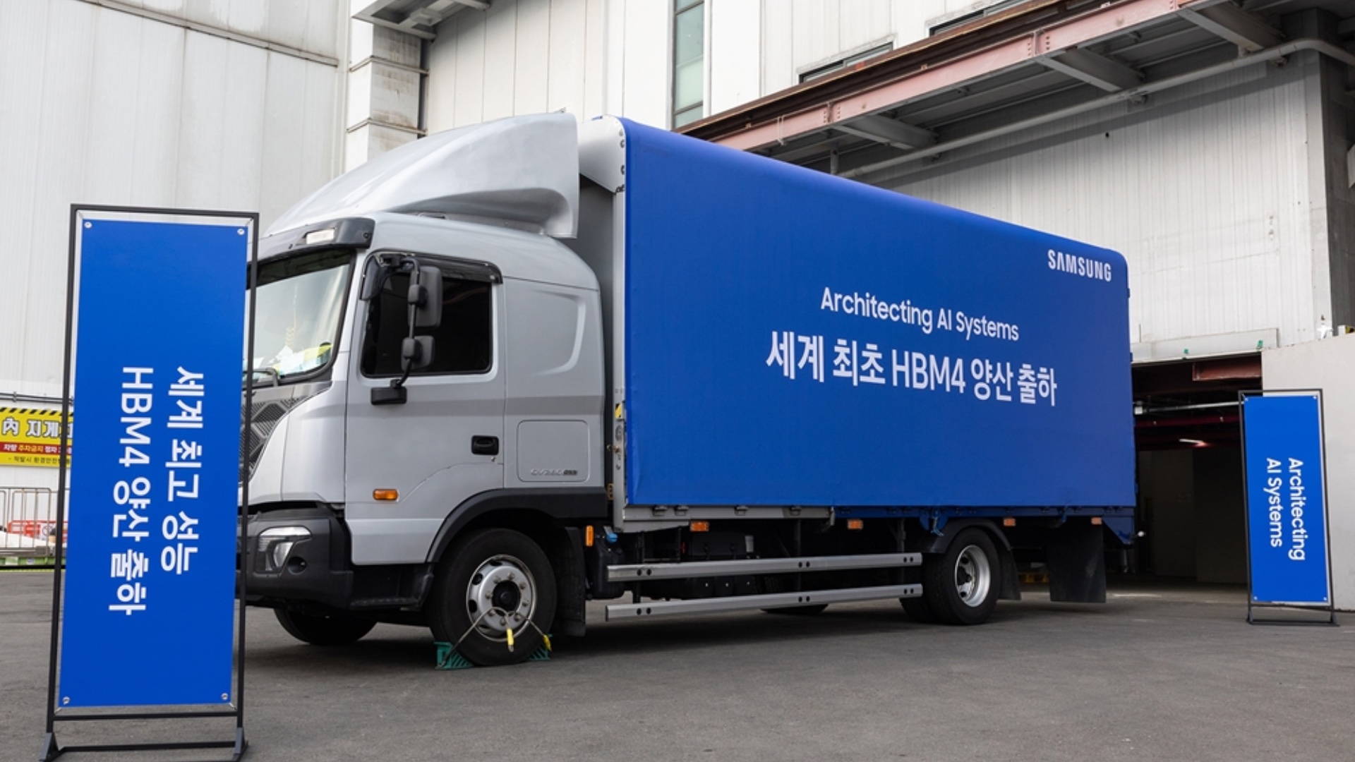
The momentum is set to continue through the end of the decade. Samsung confirmed that HBM4E chips will debut in the second half of 2026, followed by fully customized HBM chips in 2027. This customization will allow AI developers to request specific configurations tailored to their unique hardware architectures.
Hwang Sang-joon, Vice President of Memory Development at Samsung Electronics, emphasized that this milestone was achieved by moving beyond "proven processes" and embracing cutting-edge 1c DRAM and 4nm foundry tech. This aggressive approach has allowed Samsung to meet growing performance demands just as the AI industry reaches a critical fever pitch.
What makes HBM4 different from previous memory generations?
HBM4 is the sixth generation of high-bandwidth memory, offering significantly higher data transfer speeds and bandwidth compared to HBM3E. It utilizes advanced 1c DRAM and 4nm fabrication, allowing it to reach speeds of 11.7Gbps and bandwidths up to 3.3TB/s, which are essential for high-level AI calculations.
Why is Samsung's mass production of HBM4 so significant?
It marks Samsung's return to the top of the semiconductor market. After trailing behind competitors like SK Hynix and Micron, Samsung is now the first to mass-produce this specific generation of memory, securing a vital position in the supply chain for AI hardware.
What are AI accelerators and how do these chips help them?
AI accelerators are specialized hardware designed to process AI workloads efficiently. These systems require massive amounts of data to be moved quickly; HBM4 provides the necessary "highway" (bandwidth) to prevent data bottlenecks, allowing AI models to train and respond faster.
What is the maximum capacity Samsung will offer for HBM4?
While starting with 24GB and 36GB modules, Samsung has announced plans to produce 16-layer HBM4 chips that will reach a total capacity of 48GB per module to support even larger AI datasets.
When can we expect custom HBM chips?
Samsung's official roadmap indicates that custom HBM solutions, tailored to specific client needs, will begin production in 2027, following the release of HBM4E in late 2026.
🔎 Samsung’s leap into HBM4 mass production is a clear signal that the company is ready to dominate the AI era. By combining their foundry expertise with cutting-edge DRAM technology, they have created a product that not only meets but exceeds the current industry requirements. As AI continues to evolve, the underlying hardware must keep pace, and Samsung has firmly placed itself at the heart of that evolution, ensuring that the next generation of artificial intelligence is faster, smarter, and more efficient than ever before.
Post a Comment