
Next-Gen AI Power: Samsung Reveals Ultra-Fast HBM4E Memory for Supercomputers
The artificial intelligence revolution is demanding unprecedented hardware capabilities, and Samsung is stepping up to the plate. Just a month after the industry buzz surrounding the mass production of its HBM4 chips, the South Korean tech giant has officially pulled back the curtain on its seventh-generation high-bandwidth memory, the Samsung HBM4E. Unveiled at a major industry event, this new memory solution is specifically engineered to fuel the next wave of AI supercomputers and advanced neural processing.
Article Highlights:
- ✨ Samsung debuts HBM4E, the world's first seventh-generation high-bandwidth memory.
- ✨ The chip achieves massive data transfer speeds of up to 16Gbps per pin.
- ✨ Designed for integration with Nvidia’s upcoming "Vera Rubin Ultra" AI platform.
- ✨ Roadmap revealed for future HBM5 and HBM5E technologies using 2nm processes.
A Giant Leap in Bandwidth: The HBM4E Breakthrough
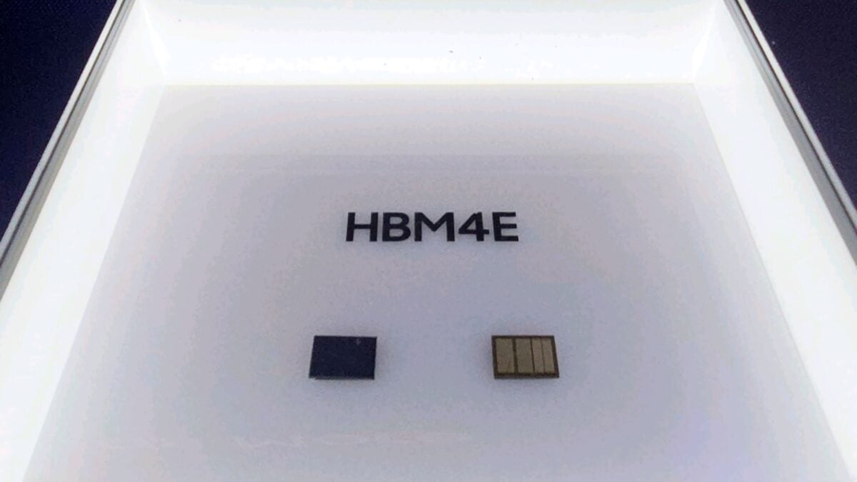
During the NVIDIA GTC 2026 event held in San Jose, California, Samsung Electronics made headlines by showcasing the HBM4E chip for the first time. By doing so, Samsung has solidified its position as a pioneer in the memory market. This seventh-generation chip is not just a minor upgrade; it delivers staggering data transfer speeds of up to 16Gbps per pin and an aggregate bandwidth reaching 4TB/s. This level of performance is essential for the massive datasets handled by modern generative AI models.
Industry experts expect the HBM4E to be a cornerstone of Nvidia’s future Vera Rubin Ultra platform. While the platform is projected to launch in the latter half of 2027, Samsung is preparing to enter mass production as early as the first half of 2027 to meet the anticipated demand for high-performance computing infrastructure.
The Roadmap to HBM5 and Beyond
Samsung isn't stopping at the seventh generation. The company explicitly outlined its vision for the future of memory technology. According to the roadmap shared at GTC 2026, Samsung intends to leverage its advanced 1c DRAM process in conjunction with a cutting-edge 2nm foundry process to develop the eighth-generation HBM5 chips. Following that, the ninth-generation HBM5E will utilize the 1d DRAM process alongside the 2nm foundry node.
A key differentiator for Samsung in this competitive landscape is its Hybrid Cap Bonding (HCB) technology. This proprietary manufacturing method is expected to provide superior thermal management and structural integrity, allowing Samsung's chips to outperform rivals in the high-stakes AI accelerator market.
Nvidia CEO Jensen Huang Endorses Samsung’s Innovation
The significance of Samsung’s progress was underscored by a visit from Nvidia CEO Jensen Huang. During his tour of the Samsung Electronics booth, Huang took a moment to personally sign an HBM4 wafer with the message “Amazing HBM4”. This public endorsement highlights the strong partnership between the two tech giants as they collaborate to build the hardware foundations of the AI era.
In addition to the HBM4E, Samsung also displayed its SOCAMM2 memory modules and the PM1763 SSD, both specifically optimized for the rigorous demands of Nvidia's AI infrastructure. These components represent a holistic approach to data center efficiency, ensuring that storage and memory can keep pace with rapidly evolving GPU capabilities.
What makes HBM4E different from standard HBM4 memory?
HBM4E is the seventh generation of high-bandwidth memory, offering significantly higher speeds and bandwidth compared to the sixth-generation HBM4. It features transfer rates of up to 16Gbps per pin and a total bandwidth of 4TB/s, making it ideal for the most demanding AI supercomputing tasks.
When will Samsung begin mass-producing HBM4E chips?
While the chips were showcased in early 2026, mass production is expected to commence in the first half of 2027. This timeline aligns with the expected launch of next-generation AI platforms like Nvidia's Vera Rubin Ultra.
How does Samsung plan to stay ahead of its competitors in the HBM market?
Samsung is focusing on advanced manufacturing processes, specifically its Hybrid Cap Bonding (HCB) technology. Additionally, the company has a clear roadmap to transition to 2nm foundry processes for future HBM5 and HBM5E generations to maintain a performance lead.
Is HBM4E compatible with current consumer PCs?
No, HBM4E is specifically designed for enterprise-level AI accelerators and supercomputers. It is integrated directly into high-performance GPUs and AI processors rather than being used as traditional RAM in consumer desktops or laptops.
🔎 The unveiling of HBM4E marks a pivotal moment in the evolution of semiconductor technology, proving that Samsung is ready to lead the charge in the AI-driven future. By pushing the boundaries of bandwidth and integrating advanced 2nm manufacturing processes, Samsung is not just keeping up with the industry; it is setting the pace. As AI models continue to grow in complexity, the collaboration between memory innovators like Samsung and platform leaders like Nvidia will be the primary engine driving global technological progress.
Post a Comment