
Samsung Shocks Tech World with Revolutionary 900-Layer V-NAND Storage Chip Prototype
Samsung, the world’s largest memory chip maker, has reportedly achieved a monumental milestone by creating the world’s first 900-layer V-NAND flash storage chip prototype. At a time when the rapid growth of artificial intelligence is driving an unprecedented demand for high-performance DRAM and NAND flash memory, Samsung is once again asserting its dominance in the semiconductor industry. This breakthrough serves as a powerful demonstration of the South Korean firm's technological prowess as it prepares to outpace global competitors.
Article Highlights
- ✨ Samsung develops the world's first 900-layer-class V-NAND flash memory prototype.
- ✨ New Cell Multi-Bonding (CMB) technology fuses two 450-layer wafers for extreme density.
- ✨ Engineered specifically to handle intensive AI computing and data workloads.
- ✨ Advanced designs significantly reduce power consumption and overall chip footprint.
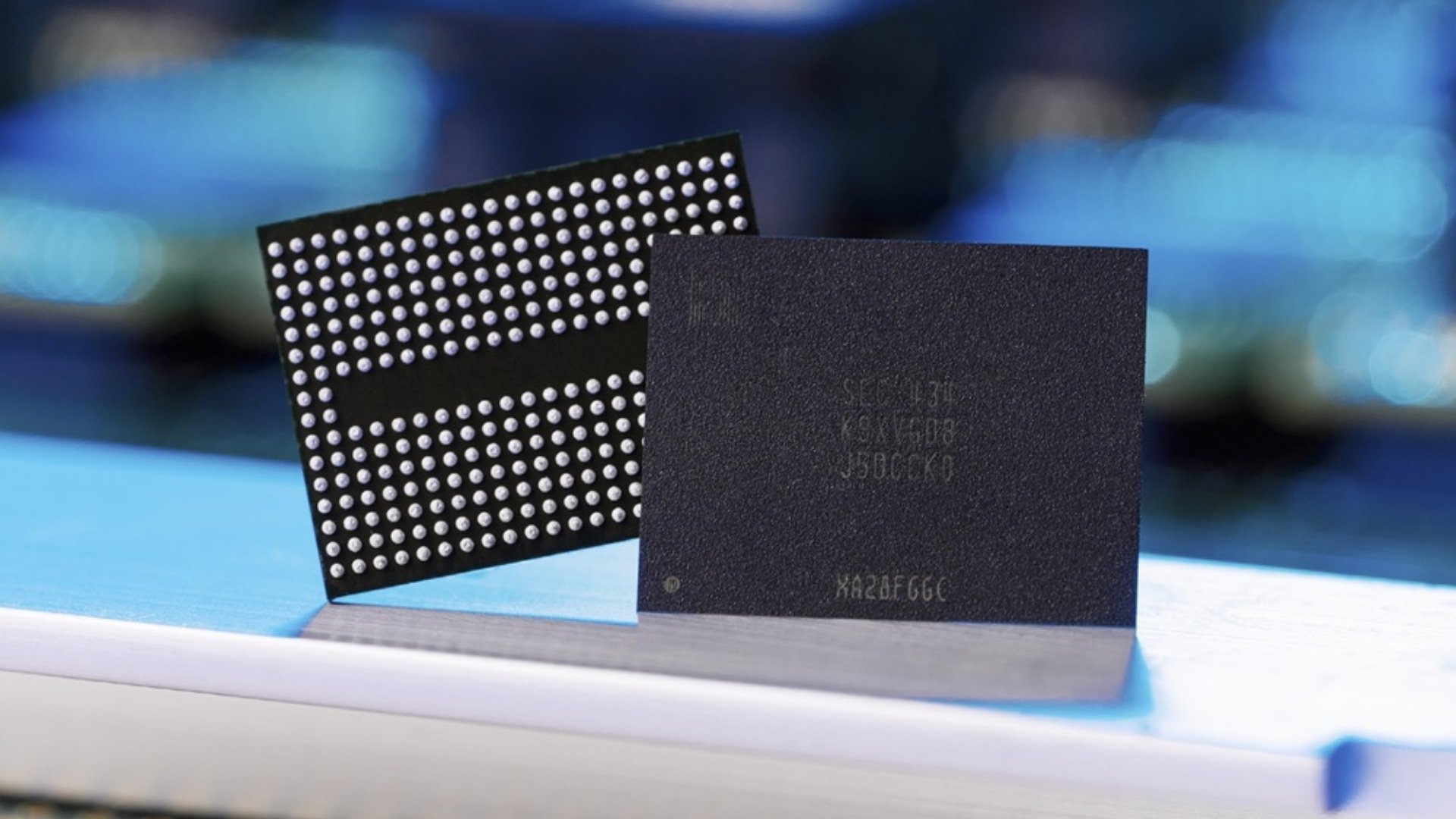
According to an exclusive report from ETNews, Samsung has successfully navigated the complexities of ultra-high stacking to produce the world’s first 900-layer-class V-NAND flash memory chip prototype. This achievement places Samsung in a unique position, far ahead of the current industry standards for storage density.
The innovative prototype utilizes a cutting-edge technology known as Cell Multi-Bonding (CMB). This process involves fusing two 450-layer cell wafers into a single, cohesive chip. By stacking NAND flash layers to this extreme height, Samsung can drastically improve storage density while simultaneously reducing power consumption. These high-density stacked structures are increasingly vital for AI computing workloads, which require massive amounts of data to be processed with maximum efficiency.
Outpacing the Competition in the AI Era
Currently, SK Hynix is recognized as a formidable leader in the high-layer NAND market with its 321-layer chips. However, Samsung’s latest breakthrough suggests it is ready to reclaim the top spot. The company is simultaneously preparing for the mass production of its 400-layer tenth-generation NAND flash chips while reaching the staggering 900-layer milestone in its research and development phase.
Samsung has a long history of innovation in this field, having been the first company to commercialize 3D V-NAND technology back in 2013. Initially, the manufacturing involved drilling and stacking microscopic holes in a single step. However, as layers reached new heights, the industry faced physical limitations such as wafer warping and stack misalignment.
To overcome these hurdles, Samsung reportedly implemented an advanced "Upper Chuck" design and "Overlay Correction" technology to ensure precision. Furthermore, improvements to the Bitline (BL) and Wordline (WL) structures have allowed for a significant reduction in both power draw and the physical size of the chip.
This acceleration in development is also a response to the growing threat from Chinese manufacturers like Yangtze Memory Technologies Co. (YMTC). YMTC has quickly closed the gap, currently mass-producing 294-layer NAND chips with heavy government backing. By reaching for the 900-layer mark, Samsung is signaling that it intends to maintain its long-term technological leadership regardless of the intensifying global competition.
What makes the 900-layer V-NAND chip so significant?
The 900-layer chip represents a massive leap in storage density. By stacking more layers, Samsung can store significantly more data in the same physical space, which is crucial for modern data centers and mobile devices.
How does Cell Multi-Bonding (CMB) technology work?
CMB technology allows Samsung to manufacture two separate 450-layer cell wafers and then fuse them together. This method helps avoid the structural instability and misalignment that often occur when trying to build a single stack of 900 layers from scratch.
Why is this technology important for Artificial Intelligence?
AI models require vast amounts of data and high-speed access to memory. High-density V-NAND provides the necessary storage capacity while reducing the energy footprint, making AI computations more sustainable and faster.
Is Samsung currently the leader in NAND flash memory?
While competitors like SK Hynix and YMTC have made significant strides with 300-layer-class chips, Samsung’s 900-layer prototype effectively doubles the current industry standard, showcasing its potential to remain the dominant force in the market.
When will we see these chips in consumer products?
As this is currently a research prototype, it may take several years before 900-layer chips reach mass production. However, the technology developed for this prototype will likely influence Samsung's upcoming 10th and 11th generation NAND products.
🔎 The development of the 900-layer V-NAND prototype is more than just a numerical milestone; it is a strategic move by Samsung to future-proof its semiconductor business. As the world moves deeper into the AI era, the demand for denser, faster, and more efficient storage will only increase. By solving the structural challenges of extreme stacking today, Samsung ensures that it will remain the primary architect of the world's digital memory for years to come.
Post a Comment