
Google’s Next-Gen AI Powerhouse: Samsung Set to Manufacture 2nm Components for Upcoming TPU
Google is aggressively advancing its proprietary hardware capabilities to lead the global Artificial Intelligence race. The tech giant is currently developing its tenth-generation AI accelerator, known as the Tensor Processing Unit (TPU). In a significant move for the semiconductor industry, Google is reportedly in high-level discussions with Samsung Foundry to utilize its cutting-edge 2nm fabrication technology for critical components of this upcoming chip.
- ✨ Google is negotiating with Samsung Foundry to manufacture parts of its 10th-generation "Icefish" TPU.
- ✨ The partnership focuses on using advanced 2nm process technology for memory I/O components.
- ✨ TSMC is expected to remain the primary manufacturer for the main compute core of the AI chip.
- ✨ This collaboration signifies a major strategic win for Samsung's foundry business in the AI sector.
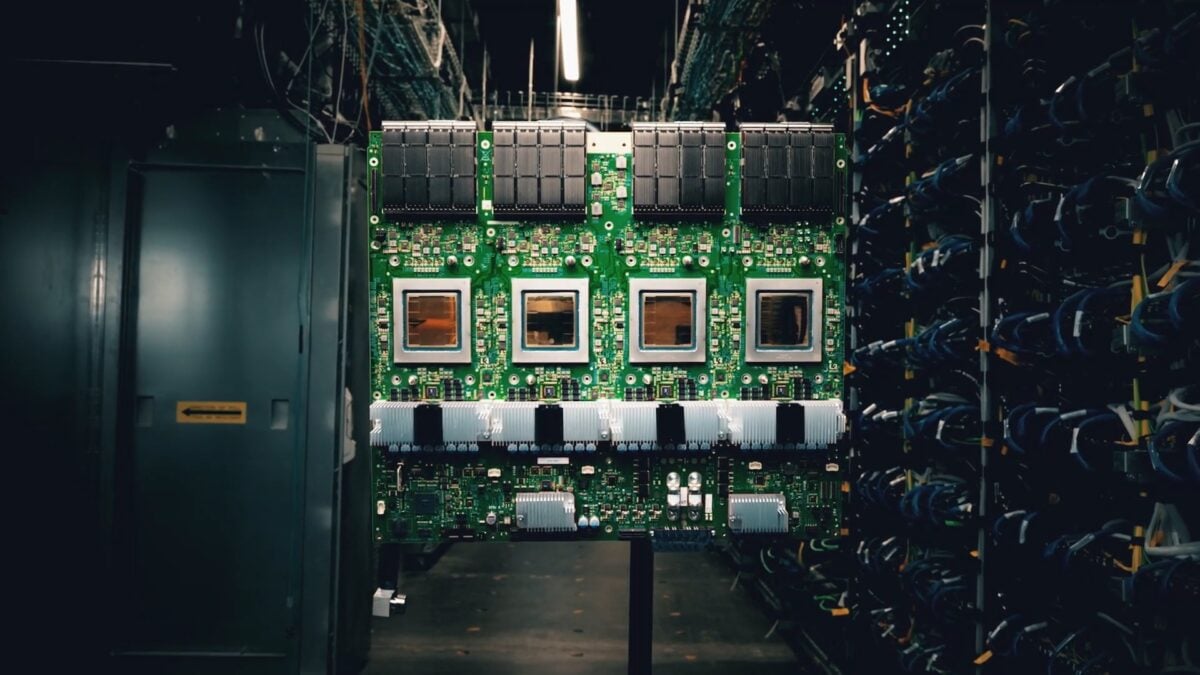
The "Icefish" Project: A Hybrid Manufacturing Strategy
According to a detailed report from The Information, Google’s tenth-generation TPU, codenamed "Icefish," might represent a shift in the company’s manufacturing strategy. While Google has traditionally relied on TSMC for its silicon needs, the "Icefish" project could see a split production model. TSMC is slated to manufacture the primary compute chiplet, while Samsung may be tasked with producing the vital component that facilitates the high-speed connection between the processor and its memory.
This potential deal is bolstered by Google’s ongoing collaboration with MediaTek on the design architecture of the upcoming TPU. For Samsung, securing a portion of Google’s TPU orders would be a massive milestone. The South Korean tech leader has been working tirelessly to attract major foundry clients to its advanced nodes, and a partnership with Google validates the maturity and efficiency of its 2nm fabrication process.
A Decades-Long Evolution of Google TPU Technology
Google’s journey with custom AI silicon began nearly a decade ago. Each generation has seen a massive leap in efficiency and processing power. To understand the scale of the upcoming v10 chip, it is essential to look at the historical progression of the TPU lineup:
| Generation | Manufacturer | Process Node |
|---|---|---|
| TPU v1 (2015) | TSMC | 28nm |
| TPU v2 (2017) | TSMC | 20nm (16nm derivative) |
| TPU v3 (2018) | TSMC | 12nm |
| TPU v4 (2021) | TSMC | 7nm |
| TPU v5e/v5p (2023) | TSMC | 5nm |
| TPU v6 (Trillium, 2024) | TSMC | Enhanced 4nm |
| TPU v7 (Ironwood, 2025) | TSMC | Advanced 3nm (N3E/N3P) |
| TPU v8t/v8i (2026) | TSMC | 2nm |
| TPU v9 (In Dev) | TSMC | Optimized 2nm |
| TPU v10 (In Dev) | TSMC & Samsung | 1.4nm (Core) + 2nm (I/O) |
Samsung’s Growing Momentum in AI Silicon
Samsung Foundry is no stranger to high-profile AI contracts. Last year, the company secured a massive $16.5 billion contract to manufacture Tesla’s AI6 chip using its 2nm node. This momentum has sparked interest from various other tech giants looking for alternatives to TSMC's crowded production lines. By diversifying its client base with names like Tesla and potentially Google, Samsung is positioning itself as a formidable pillar in the global semiconductor supply chain.
The South Korean firm recently expressed optimism regarding its advanced fabrication processes, noting that it expects to secure a higher volume of orders as the demand for specialized AI hardware continues to skyrocket. For more details on the original report, you can visit the following link:
What exactly is a Google TPU?
A Tensor Processing Unit (TPU) is an AI accelerator application-specific integrated circuit (ASIC) developed by Google specifically for machine learning. Unlike general-purpose CPUs or GPUs, TPUs are optimized to handle the massive mathematical workloads required for neural network training and inference.
Why is Google involving Samsung in the TPU v10 production?
As manufacturing nodes become smaller and more complex, companies often look to diversify their supply chains. Samsung’s 2nm technology offers a competitive solution for memory I/O components, allowing Google to leverage the strengths of both Samsung and TSMC to optimize performance and ensure production capacity.
What is the significance of the 2nm process?
The 2nm process refers to the size of the transistors on the chip. Smaller process nodes allow for more transistors to be packed into a smaller area, which typically results in higher processing speeds, better energy efficiency, and reduced heat generation—all of which are critical for AI data centers.
When will the tenth-generation TPU be released?
While the TPU v10 is currently under development, industry experts suggest it could debut as early as 2027 or 2028, following the rollout of the TPU v8 and v9 series which are slated for the next few years.
Will this affect Samsung Galaxy smartphones?
While the TPU is a server-side chip for data centers, the advancements Samsung makes in 2nm manufacturing for Google will likely trickle down to its consumer-grade Exynos and Snapdragon processors, leading to more powerful and efficient mobile devices in the future.
🔎 In conclusion, the potential partnership between Google and Samsung Foundry for the 10th-generation TPU marks a pivotal moment in the evolution of AI hardware. By integrating Samsung’s 2nm technology into its "Icefish" project, Google is ensuring it has the technological infrastructure necessary to power the next era of machine learning. For Samsung, this deal represents a significant step forward in its goal to become the world’s leading foundry, proving that its advanced nodes are ready for the most demanding applications in the tech industry today.
Post a Comment