
Samsung Introduces Groundbreaking zHBM Memory Concept Delivering Eight Times the Speed of HBM5
Samsung has taken a monumental step forward in high-performance computing by unveiling an innovative memory chip architecture known as zHBM. Tailored specifically to support next-generation artificial intelligence infrastructure, this advanced design promises to shatter current bandwidth and density limitations, completely transforming how data flows within modern data centers.
- ✨ Samsung revealed zHBM, a revolutionary Z-axis High Bandwidth Memory concept engineered for high-performance servers and AI data centers.
- ✨ The revolutionary architecture is designed to deliver roughly eight times faster speeds and over ten times the memory density compared to upcoming HBM5 hardware.
- ✨ Thermal resistance is reduced by 50%, while energy efficiency is tripled through advanced vertical stacking methodologies.
- ✨ While commercial production has not been finalized, industry timelines point toward a rollout following the adoption of HBM5 technologies around 2028.
Redefining AI Hardware Architecture with Z-Axis Integration
Samsung, recognized globally as the world's biggest memory chip maker, officially introduced its breakthrough zHBM concept. Standing for Z-axis High Bandwidth Memory, this technology aims to resolve the severe performance bottlenecks that current enterprise infrastructure encounters when processing massive artificial intelligence workloads.
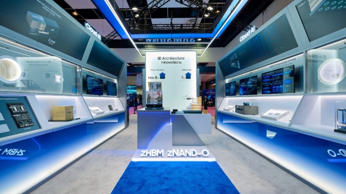
Showcased during the Future of Memory and Storage (FMS) 2026 exhibition in Santa Clara, California, the zHBM concept alters conventional chip placement strategies. Instead of arranging memory components horizontally beside an HBM processor on a shared interposer layer, zHBM stacks the memory directly on top of the AI accelerator.
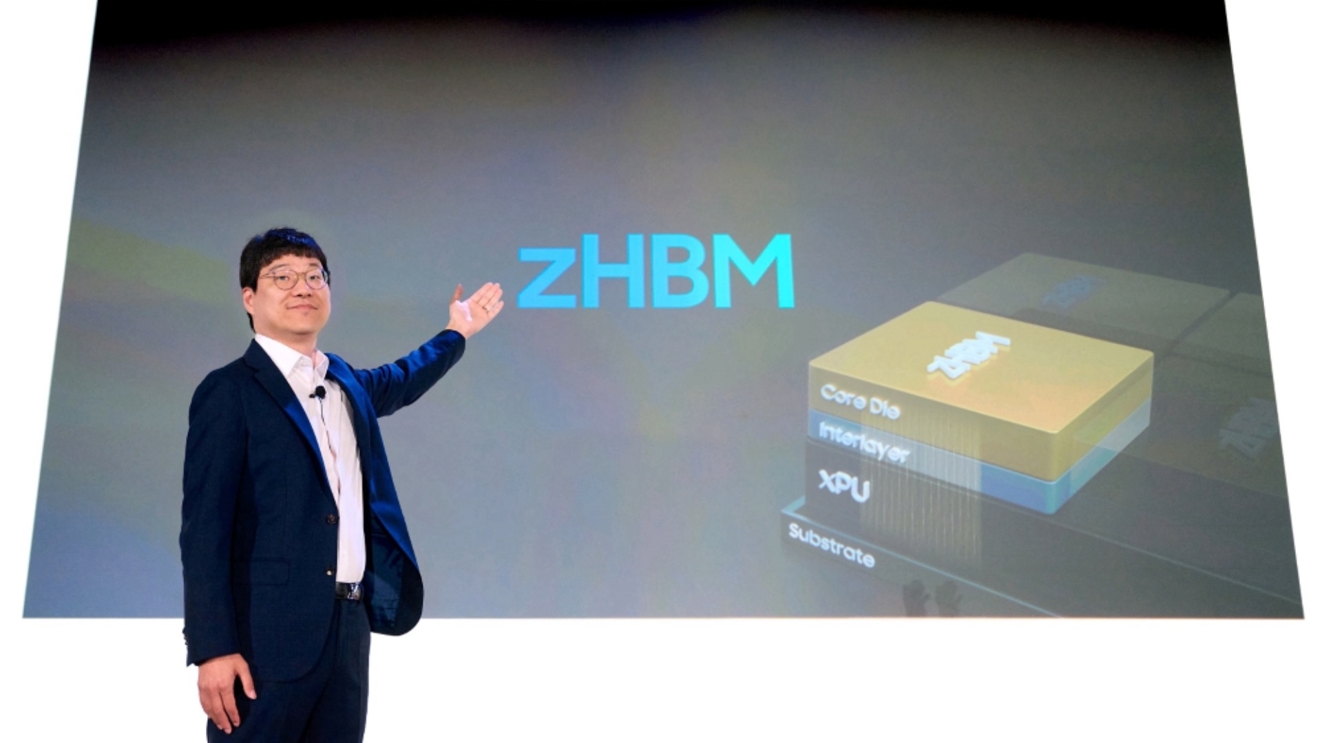
By shortening the physical pathway between the compute engine and the storage layer, data-transfer speeds increase exponentially. Samsung projects that zHBM configurations can achieve roughly eight times the speed and ten times the density offered by standard HBM5 chips, pushing the boundaries of what enterprise servers can accomplish.
Beyond raw speed, the architecture features cutting-edge wafer-bonding technologies that deliver three times the energy efficiency while cutting thermal resistance in half compared to legacy configurations. Furthermore, the modular design supports customized layers between the processor and memory stack, paving the way for hyper-specialized enterprise deployments.
What is the primary architectural advantage of Samsung's zHBM concept?
The zHBM architecture stacks memory chips directly on top of the AI accelerator along the vertical Z-axis, drastically shortening the physical distance between processor and memory compared to traditional horizontal layouts.
How much faster is zHBM expected to be compared to HBM5?
Samsung claims that zHBM can achieve approximately eight times faster data-transfer speeds and more than ten times the memory density of upcoming HBM5 hardware.
What thermal and energy benefits does zHBM provide?
The innovative design delivers triple the energy efficiency and reduces thermal resistance by 50% compared to conventional memory architectures.
When can the market expect commercial zHBM hardware?
Samsung has not specified an exact release window, but industry projections indicate that commercial availability will likely follow the widespread rollout of HBM5 chips post-2028.
🔎 Ultimately, Samsung's zHBM concept represents a visionary leap forward for high-performance hardware engineering. By addressing core thermal, speed, and density limitations through creative vertical integration, Samsung is laying a robust foundation for the next generation of scalable, enterprise-grade AI infrastructure.
Post a Comment