
Samsung Enhances Manufacturing Power with Advanced ASML Equipment
Samsung is upgrading its advanced semiconductor production by strengthening its alliance with Dutch equipment giant ASML. This strategic move introduces cutting-edge lithography technology to manufacture powerful logic and memory chips designed specifically to meet the growing demands of the modern artificial intelligence era.
- ✨ Samsung is expanding its collaborative partnership with ASML to deploy High-NA EUV machinery for next-generation chip production.
- ✨ The integration of advanced 12-inch photomasks helps streamline fabrication productivity, reduce manufacturing costs, and eliminate node constraints.
- ✨ Samsung has officially announced plans to implement High-NA EUV equipment for high-volume DRAM manufacturing by the year 2028.
Article Summary:
Samsung is scaling up its semiconductor manufacturing capabilities by partnering with ASML to adopt High-NA EUV lithography and 12-inch photomasks, paving the way for advanced logic chips and mass DRAM production by 2028.
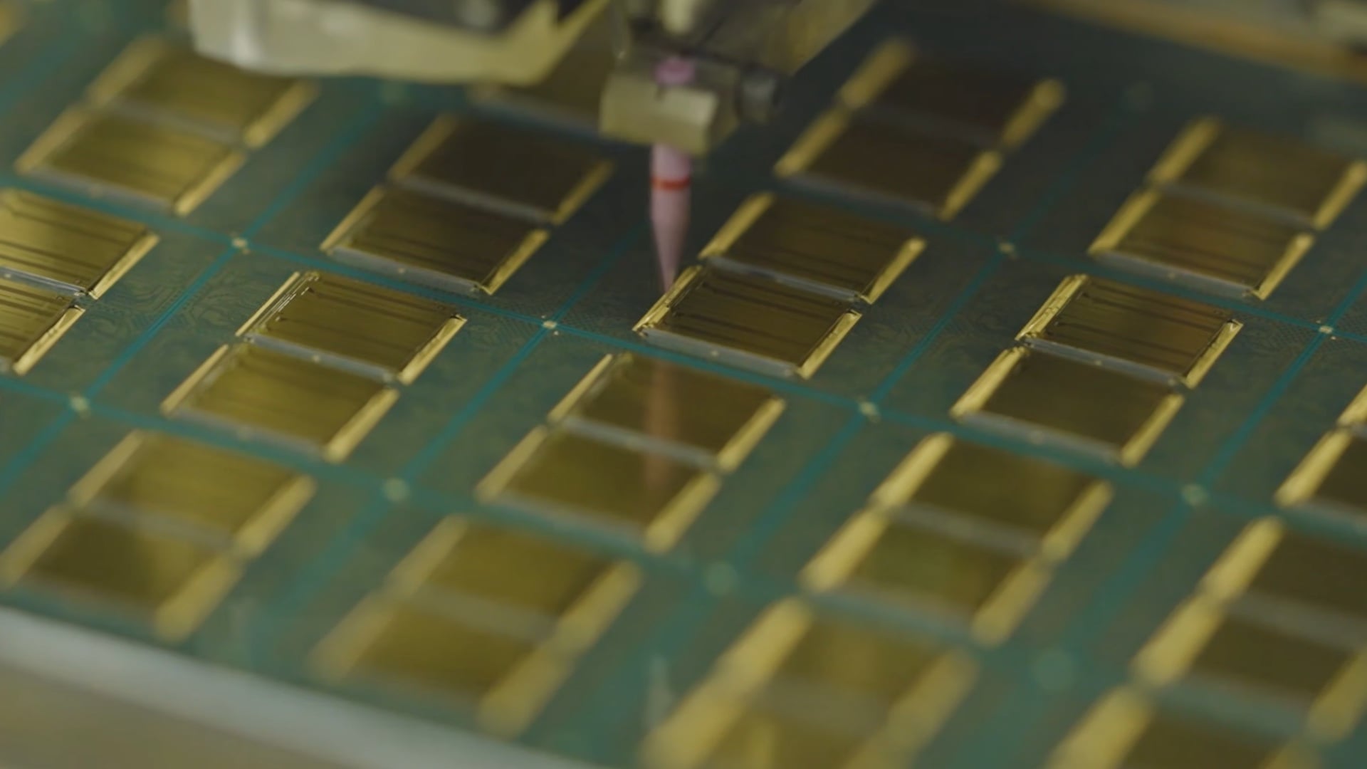
Driving Innovation in Semiconductor Fabrication
As one of the world's largest semiconductor chipmakers, Samsung continually enhances its technical capabilities to stay ahead of industry demands. By utilizing ASML's state-of-the-art High-NA Extreme Ultraviolet lithography equipment, the company aims to optimize production efficiency for advanced Samsung Foundry nodes.
Furthermore, the transition to modern 12-inch photomasks replaces legacy standards, improving overall yield and removing manufacturing limitations. Leadership at Samsung Electronics emphasizes that these breakthroughs build a solid foundation for future hardware developments in AI technology.
What advantages do High-NA EUV machines bring to Samsung?
High-NA EUV equipment allows chipmakers to print finer circuit patterns with extreme precision, greatly improving the performance, speed, and energy efficiency of modern semiconductors.
When will Samsung start using High-NA EUV for memory production?
Samsung has announced plans to incorporate High-NA EUV technology into high-volume DRAM manufacturing by 2028, marking an industry-first milestone.
Why is the industry shifting to 12-inch photomasks?
The adoption of next-generation 12-inch photomasks helps boost fab productivity, lower overall manufacturing costs, and eliminate stitching constraints on leading-edge semiconductor nodes.
How does this partnership impact AI development?
The AI era demands massive computational power and efficiency. Upgrading fabrication infrastructure enables the production of faster and more reliable hardware capable of handling complex AI workloads.
🔎 Conclusion: Samsung's ongoing collaboration with ASML represents a monumental step forward for advanced hardware manufacturing. By adopting next-generation fabrication tools and pioneering high-volume DRAM production methods, Samsung is well-positioned to lead the next generation of semiconductor innovation.
Post a Comment