
Samsung Adapts Strategy by Outsourcing Nvidia's Custom HBM4E Base Dies to TSMC
Samsung has traditionally handled the manufacturing of base dies for its high-bandwidth memory chips entirely in-house. However, recent reports indicate that the company has agreed to utilize rival TSMC's 3nm manufacturing process for customized chip architectures tailored specifically for high-performance computing infrastructure.
Key Takeaways
- ✨ Samsung has accepted Nvidia's specifications to adopt TSMC's advanced 3nm fabrication for specialized HBM4E base dies.
- ✨ The core memory components will still rely on Samsung's proprietary sixth-generation 1c production nodes.
- ✨ Standard memory modules meant for alternative corporate partners will remain entirely within internal production lines.
- ✨ Samsung Foundry is actively testing redundant production capabilities to prevent any downstream supply chain interruptions.
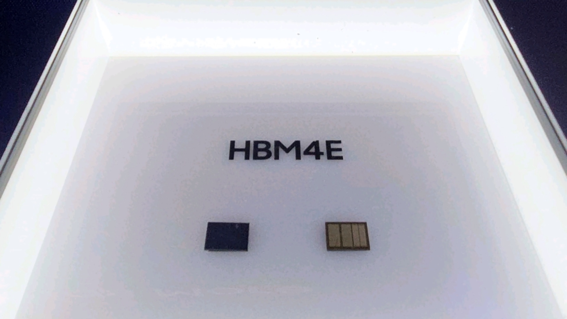
Shifting Dynamics in High-Bandwidth Memory Manufacturing
Samsung generally follows an integrated turnkey manufacturing philosophy for its Samsung Memory products. This means that both the core memory stack and the companion system-on-chip base layers are normally fabricated directly within proprietary Samsung Foundry cleanrooms. Despite this long-standing practice, hardware requirements driven by major technology developers have forced a strategic adjustment regarding custom component integration.
Industry partners requested that leading semiconductor fabricators leverage TSMC's refined 3nm manufacturing capabilities for specialized base layer wafers. Adopting this unified approach guarantees predictable operational performance and streamlines validation workflows for next-generation hardware environments.
Balancing External Partnerships and In-House Production
Although Samsung has previously partnered with external foundries for specific packaging procedures, utilizing a direct competitor for advanced wafer fabrication marks a notable shift in operational policy. Even with this outsourcing agreement for customized components, the underlying core storage layers will continue to utilize Samsung Device Solutions in-house 1c manufacturing technology.
Concurrently, standard memory components destined for other commercial hardware ecosystems will maintain strict domestic production pipelines. Furthermore, internal validation teams are conducting parallel testing to ensure that proprietary fabrication facilities can serve as a dependable secondary source should any unexpected supply chain bottlenecks arise.
Why is Samsung outsourcing part of its chip production to TSMC?
Samsung agreed to this layout modification to satisfy specific performance parameters requested by hardware architects for specialized enterprise infrastructure chips.
Will all memory chips be manufactured using TSMC nodes?
No, only customized base dies for specific enterprise applications will utilize TSMC's nodes, while standard memory architectures remain within internal production facilities.
What node technology does Samsung use for the core memory layers?
The core storage components will continue to be fabricated using Samsung's in-house sixth-generation 1c production process.
Does Samsung have a contingency plan for production issues?
Yes, the firm is actively evaluating its internal fabrication lines to act as a reliable backup plan in case external production capacities experience limitations.
🔎 Ultimately, this strategic compromise demonstrates a pragmatic shift in the semiconductor industry, allowing major manufacturers to balance competitive rivalries with the rigorous demands of modern enterprise-grade hardware development. By collaborating across manufacturing ecosystems, technology leaders can successfully navigate complex production challenges while keeping high-performance hardware pipelines moving forward.
Post a Comment